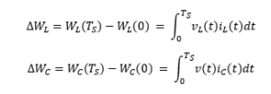
The application of power electronics to communications devices has to do with the processing of the electrical input power using semiconductor devices and reactive elements.
Thus, the raw input power is processed according to a control input that conditions the output power. This conditioning can be carried out by DC/DC converters – that convert the DC input voltage into another DC voltage with different magnitude and possibly isolated or even inverted polarity or through AC/DC converters that produce DC voltage from an AC input voltage.
A high efficiency level (of over 85%) is essential in all power applications. The reason for this is not just a question of cutting the electric bill, nor the noble aim of respecting the environment, but rather that the internal power dissipation of a converter generates heat that has to be drawn out. If the converter output power is high, the losses will also be high according to the ratio:
![]()
Such losses, in turn, lead to costly and complex cooling systems, high internal operating temperatures for devices, and, consequently, reduced reliability. Thus, increasing efficiency is a primary design objective for communications devices.
How can we build a circuit that changes the voltage without dissipating power or dissipating a minimum power? We do this, of course, by using capacitors and magnetic devices like coils and transformers; since “ideally” they do not dissipate power, but rather store energy to be released at another time. We also use semiconductor devices in the switched mode. When one of these components operates in the OFF state, its current is zero, as is its dissipation. When it operates in the ON state, its voltage drop is small and hence its power dissipation is also small. In summary, capacitors, coils and transformers, as well as semiconductor devices operated in the switched mode are the elements we have at our disposal for synthesizing high efficiency converters.
Let´s briefly look at the fundamentals of the process in the case of the converter in Figure 1 which raises the output voltage above the input (boost converter). Before doing this, however, we need to briefly explain the operation of the X1 “spdt” block in Figure 1. This represents an ideal switch that connects the IN input either to GND or to the LOAD (represented by the 12 ohm R1 resistance), under the control of the V2 signal, so that when the voltage at the “+” terminal is higher than in the “-” terminal, the switch is in position 1 and the coil current flows through the null impedance of the “spdt” to ground. At a given instant, the voltage between the “+” and “-” terminals drops down to zero, which is when the switch changes to position 2 and the coil current flows towards C1 and R1. This switch-changing process (from position 1 to 2 and 2 to 1) takes place periodically at the frequency fS (1/10 us in our example) as Figure 2 shows for two periods. The percentage of time the switch is in position 1 during each period is called duty cycle and is represented as D.
Finally, let us consider three basic physical facts that we will use in due course.
- The first is that the energy stored by a coil depends on the square of the current flowing through it, and that of a capacitor, on the square of the voltage at its terminals. Therefore, the current variation, in the first case, and of the voltage variation, in the second, cannot be instantaneous (as this would require infinite power).
- The energy variation stored by a coil or capacitor in a cycle will be equal to the difference between the final and initial energy. The general expressions are:
- The third is that if the converter natural time constants are much longer than the switching period Ts (10 us in our example), it can be assumed that any magnitude x(t), whether current or voltage, will vary very little in the switching time period, or in each subinterval, and, consequently, the actual signal will consist of a desired continuous component, plus a small undesired ripple This assumption, known as the small ripple approximation, is equivalent to:
![]()
Going back to the circuit in Figure 1, upon reaching steady state, it reaches a situation of equilibrium in which the power stored by coils and capacitors during a cycle must equal what’s discharged. Therefore, by equating the general expressions presented above to zero and applying the small ripple approximation (identified by an approximately equal sign in front of the expression), we see that the average value of the coil voltage and the increase of the capacitor charge must be zero:
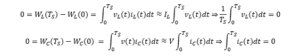
Having established the above principles, denominated inductor volt-second balance and capacitor charge balance, we apply them to our circuit during a switching period once equilibrium is reached.
With the switch in position 1, the voltage at the coil is:
![]()
And in position 2:
![]()
As far as the current through the capacitor is concerned, with the switch in position 1, we have:
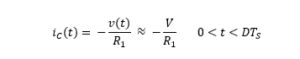
And in position 2:

Thus we obtain the coil voltage and the capacitor current in each of the two subintervals that make up a switching cycle. However, they are not independent because they need to satisfy the volt-second balance and capacitor charge balance conditions:
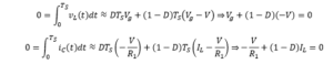
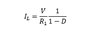
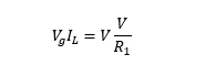
If we simplify we get the expression relating the converter’s output voltage to the input:

And the expression relating the current flowing through the coil to the output current that is delivered to the load R1:
These two expressions allow us to verify that the input power is transferred to the output, without loss:
Finally, applying the obtained formula to the 30% and 70% duty cycle cases, we see how an ideal boost converter is capable of stepping up the voltage from a 12V source to any other value that might be necessary in the equipment (such as 17.1V or 40V) without loss; and that these theoretically obtained values, coincide with the results shown in Figure 3 calculated using a simulation tool.
| D | V (volt) |
| 0.3 (30%) | 17.1 = 12 / (1 -0.3) |
| 0.7 (70%) | 40.0 = 12 / (1- 0.7) |
In conclusion, Teldat devices that are equipped with the latest technology have multiple DC/DC converters that convert a 12 volt input voltage into other normally smaller voltages (buck converters); thus, the Teldat-iM8 is fitted with converters that generate: +3.3V for LVTTL logic; +2.5V and +1.8V for Ethernet and SFP, +1.35V for DDR3L, SGMII, SATA and PCI Express and +1.0V for processor cores. In all cases, their performance is close to or above 90%.

Figure 1. Ideal boost converter schematic

Figure 2. V2 control signal for 30% (green) and 70% (blue) duty cycles. Switch X1 is in position 1 when the V2 level is above 0.9V and in position 2 when it is at 0.0V.

Figure 3. Converter output voltage at capacitor C1 terminals for 30% (green) and 70% (blue) duty cycles.